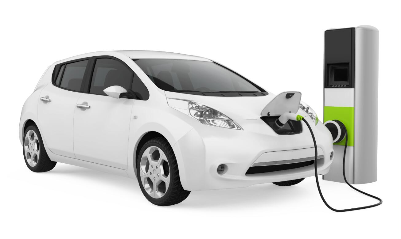
With exponential growth of electric vehicles (EV) in many countries, publicly accessible EV chargers are increasingly
needed to provide the same level of convenience and accessibility as for refueling conventional vehicles.
There are two main types of EV chargers, namely charging piles and charging stations. Charging piles are commonly installed
in residential area, commercial buildings (such as shopping malls and hotels), and public locations such as car parks. The
input end of the charging pile is directly connected to the AC power grid, and the output end is equipped with a charging
plug for charging various electric vehicles. These charging piles are usually designed to output either single-phase or
three-phase AC voltage, with power output usually ranging from 3kW to 22kW. The AC output is then converted into DC voltage
by the OBC (on-board charger) inside the EV to charge the on-board battery.
The input of charging station, on the other hand, is usually connected to the provincial national electric power grid
while the output end is equipped with a bulky charging plug with either AC or DC output voltage. Charging station with
DC output (also known as 'off-board charger') directly charge the on-board battery storage without the OBC. Such charging
stations are typically designed to support high charging rate of 60/120/200kW or even higher.
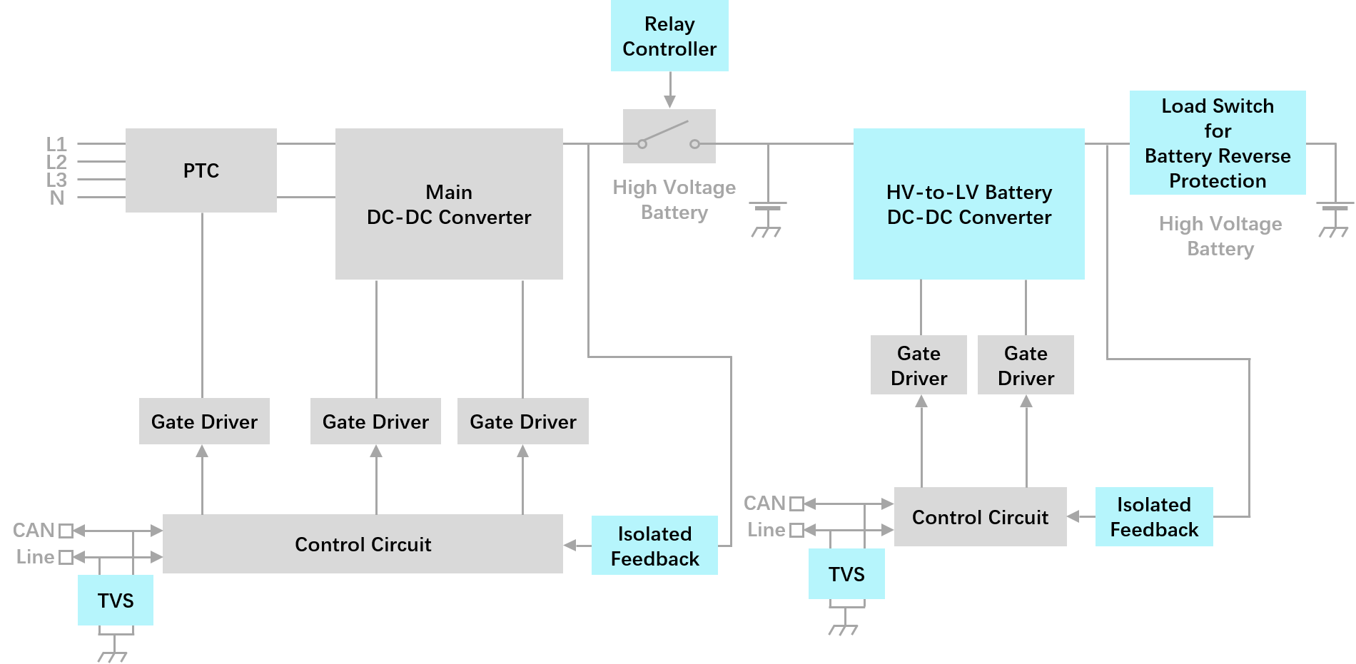
In both OBC and off-board charger, there are two key power stages, PFC and DC/DC converter. The PFC (power factor correction)
stage provides high power factor and low total harmonic distortion (THD) to reduce the reactive power needed from the power grid.
Meanwhile it provides a regulated high DC voltage to the DC/DC converter, where the DC voltage is converted into the voltage level
required for charging the EV battery. The output voltage and current of the DC/DC converter vary over time depending on the overall
health and charge level of the on-board battery.
Circuit diagram of EV charger
JJM offers a wide range of power discrete semiconductor components for the PFC and DC/DC converter.
These include bridge rectifier, FRED (fast recovery epitaxial diode), Schottky diode, power MOSFET, and optocouplers.
JJM also offers wide range of TVS (transient voltage suppressor) and ESD protection for the CAN communication port and
key components such as MOSFETs.